SK Hynix could be held as an everyday hero with its latest 238-layer 4D NAND Flash memoryt announcement. Why? Because it’s promised to bring the flash new Flash memory straight to consumer SSDs for our home rigs.
Competitor, Micron, on the other hand, recently announced its own new 232-layer memory will be limited to enterprise machines on launch. Basically, the common folk’s memory solution is set to be more impressive than what the corpos will be packing.
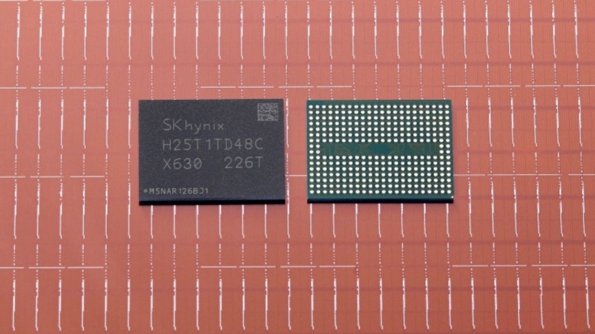
Enter the world’s first 512Gb (that’s gigabit, not gigabyte) triple level cell (TLC) 4D NAND flash memory—coming right to our desks some time in early 2023. SK Hynix has aimed for the highest NAND stack ever designed, after the company’s successes with its 176-layer NAND memory solution, back in late 2020.
Although it’s got 62 layers on its predecessor, the design still manages to fit into an impressively minimal form factor. In fact, it’s the smallest NAND product we’ve seen, though SK Hynix has managed to improve on the current standard’s power efficiency, data transfer speeds, and all-around productivity.
A SK Hynix newsroom release (opens in new tab) outlines the new design’s overall productivity has increased by 34% over the previous generation’s 176-layer model, along with 50% faster data-transfer speeds of 2.4Gb per second over the previous 1.6Gbps. It’s also promising 1Tb versions next year—that’s a mighty 128GB of storage on a single tiny chip.
The company has made some steady improvements compared to its last generational leap, with its 176-layer tech only touting a 33% increase to data-transfer (opens in new tab) speeds over its 128-layer technology.
‘If you think about it, everything is 4D’—SK Hynix’s marketing department, probably
What might be tripping some of you up is where SK Hynix gets off on using the term 4D (opens in new tab). Like, does the company really think there’s some magical fourth dimension helping them make more efficient tech? Of course not. The terminology refers to the use of CTF (charge trap flash) designs in their layering, which involves tucking its periphery circuitry under its cell stack, known rather inventively as periphery under cell (PUC) tech.
This isn’t a new thing by any stretch; Samsung, Toshiba, and Western Digital have all been using this method for some time. What is new is just how many layers the company has managed to jam into such a tiny space.
We’ll have to wait and see if 2023 is the year that demand for SSD coolers skyrockets, but until then we can only thank SK Hynix for putting the average PC gamer first, as opposed to reaching first for servers, as Micron is (opens in new tab).